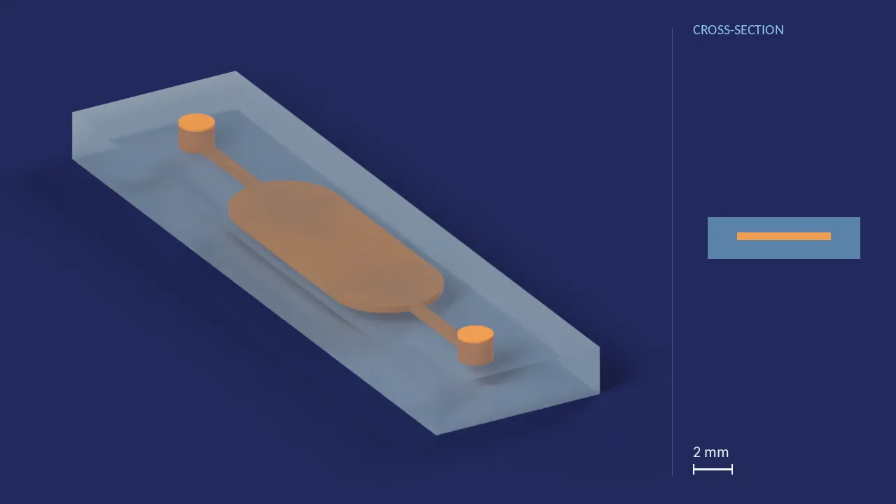
Internal geometry — X-ray
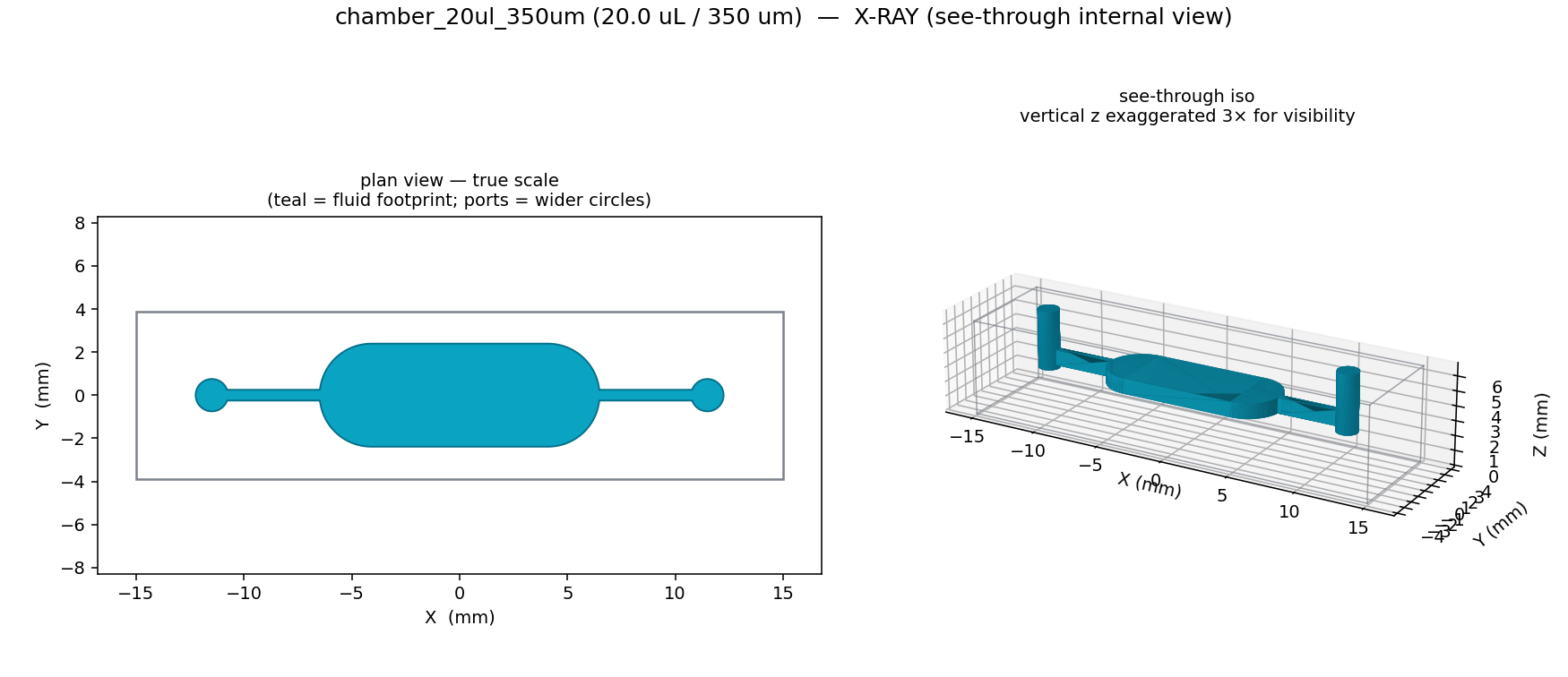
See-through internal view. Left: fluid footprint in plan, true scale (teal); ports show as the wider circles. Right: isometric of the internal void, vertical z exaggerated 3× for visibility. The exterior is an opaque solid block — this is what is inside it.
Download: PNG (x-ray)
Longitudinal section & exterior
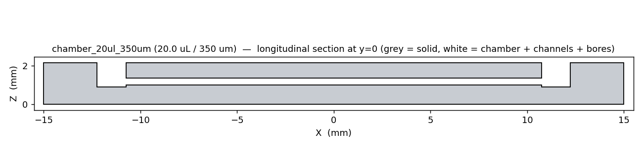
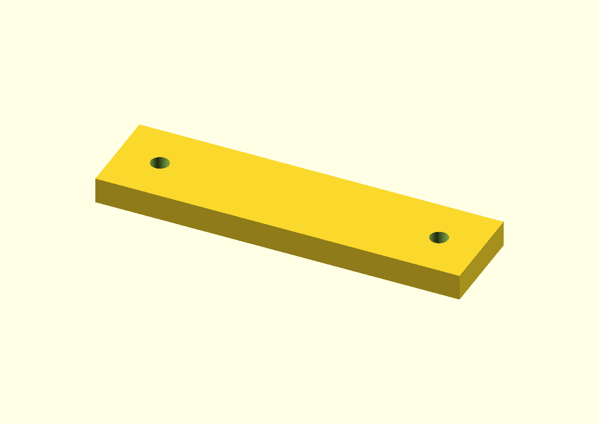
Longitudinal section at y=0 (left): grey = solid, white = fluid voids. Exterior isometric (right): the outside of the CAD model, drawn opaque. Click either for full resolution.
Download: PNG (section) · PNG (top) · PNG (iso)

Description
A single monolithic resin-SLA block with one 20 µL, 350 µm-deep stadium reaction chamber, two straight 0.5 mm feed channels on the same floor, and two Ø1.5 mm vertical access bores to the top surface. Footprint 29.9782 × 7.7809 × 2.15 mm.
The target is a 20 µL chamber, 350 µm deep. The model reproduces it exactly — the mesh measures 19.9955 µL, -0.022% from target. The stadium is sized by an inverse-solve: area = volume ÷ depth = 57.1429 mm², then a width chosen to hold the same stadium aspect ratio (L/w = 2.7146) as the 20 µL chamber chip, 500 µm deep — that is w = √(A/2.5) = 4.7809 mm, giving a chamber length of 12.9783 mm.
Verification
| metric | value |
|---|---|
| Chamber volume — target | 20 µL |
| Chamber volume — measured on the model's mesh | 19.9955 µL (-0.022% vs target) |
| Chamber depth — target | 350 µm |
| Chamber area (volume ÷ depth) | 57.1429 mm² |
| Chamber stadium (L × w) | 12.9783 × 4.7809 mm |
| Stadium aspect ratio (L/w) | 2.7146 — held from chamber_20ul_500um so the family is geometrically similar |
| Footprint (L × W × H) | 29.9782 × 7.7809 × 2.15 mm |
| Chip watertight | True |
| Chip Euler number | 0 — genus-1: one cavity, two vents |
| Void connected bodies | 1 — chamber and both bores continuous |
| Min feature vs Phrozen 12K X (px_min = 350/19) | 18.42 px |
| Min feature vs Phrozen 12K Y (px_min = 350/24) | 14.58 px |
| Min feature vs BYU Nordin (px_min = 350/7.6) | 46.05 px |
All geometry checks run with trimesh (merged vertices) on the exported STLs. See the bundled README for the full method. The minimum-feature rows are pixel counts; for each printer’s process limits, see Hardware and process.
Cross-family consistency. This inverse-solve reproduces the target volume to -0.022% here, and to within 0.023% on every chamber in this family — the 2.5, 5, 10 and 50 µL chambers and the 20 µL chambers 350 and 500 µm deep. Agreement to three decimal places across a 20× volume range shows the solve behaves identically at every scale.
Print adaptation
Target dimensions are what the design aims at; drawn dimensions are what its CAD model is drawn at. Where the two are the same number, no feature was resized to print.
Credits
Design: Ali Tahmasbizadeh, Gale Lab, University of Utah.
Files to download
- SCAD
chamber_20ul_350um.scad12.1 KBDownload - STL
chamber_20ul_350um.stl210.8 KBDownload - STL
void_chamber_20ul_350um.stl207.9 KBDownloadFor inspection, not for printing: the fluid network, every space that holds liquid, as a solid. - PNG
chamber_20ul_350um_xray.png147.0 KBDownload - PNG
chamber_20ul_350um_section.png18.6 KBDownload - MD
README.md1.4 KBDownload